Fluid Jet polishing has enabled LightMachinery to produce large thin optics with less than 10nm of thickness variation. These techniques can be applied to a wide variety of optical and semiconductor materials including Fused Silica, BK7, Silicon, Silicon on Insulator, SOI, Germanium, Zinc Selenide, Calcium Fluoride and Magnesium Fluoride.
Conventional polishing relies on controlling the shape of a polishing lab to adjust the entire surface of an optical element. In the hands of one of LightMachinery's master polishers, conventional hand polishing can achieve remarkable results but it has limitations. Conventional polishing can only adjust the basic parameters of wedge, sphere and astigmatism.
Fluid jet polishing utilizes a small computer controlled polishing tool that removes material in a very slow but predictable pattern. Advanced software developed by LightMachinery enables the correction of wavefront errors to remove nanometers of material and achieve surfaces that are very close to perfect. Fluid jet polishing is enabling optical, nanostructural, microfluidics, Silicon on Insulator (SOI), MEMS, and semiconductor projects that were previously considered to be impossible.
If your application requires truly flat smooth surfaces, uniform thickness or surfaces with arbitrary aspheric shapes then contact our staff to discuss your needs.
FLAT, UNIFORM THICKNESS, THICK OR THIN, ROUND OR SQUARE
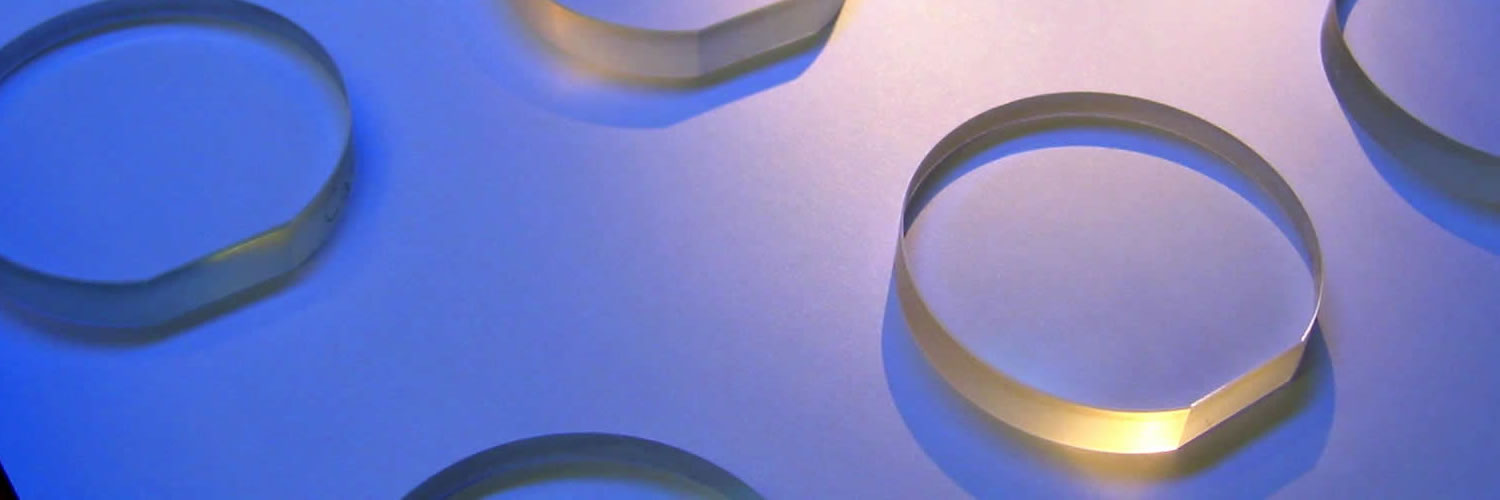
A sample of the flat optics produced at LightMachinery


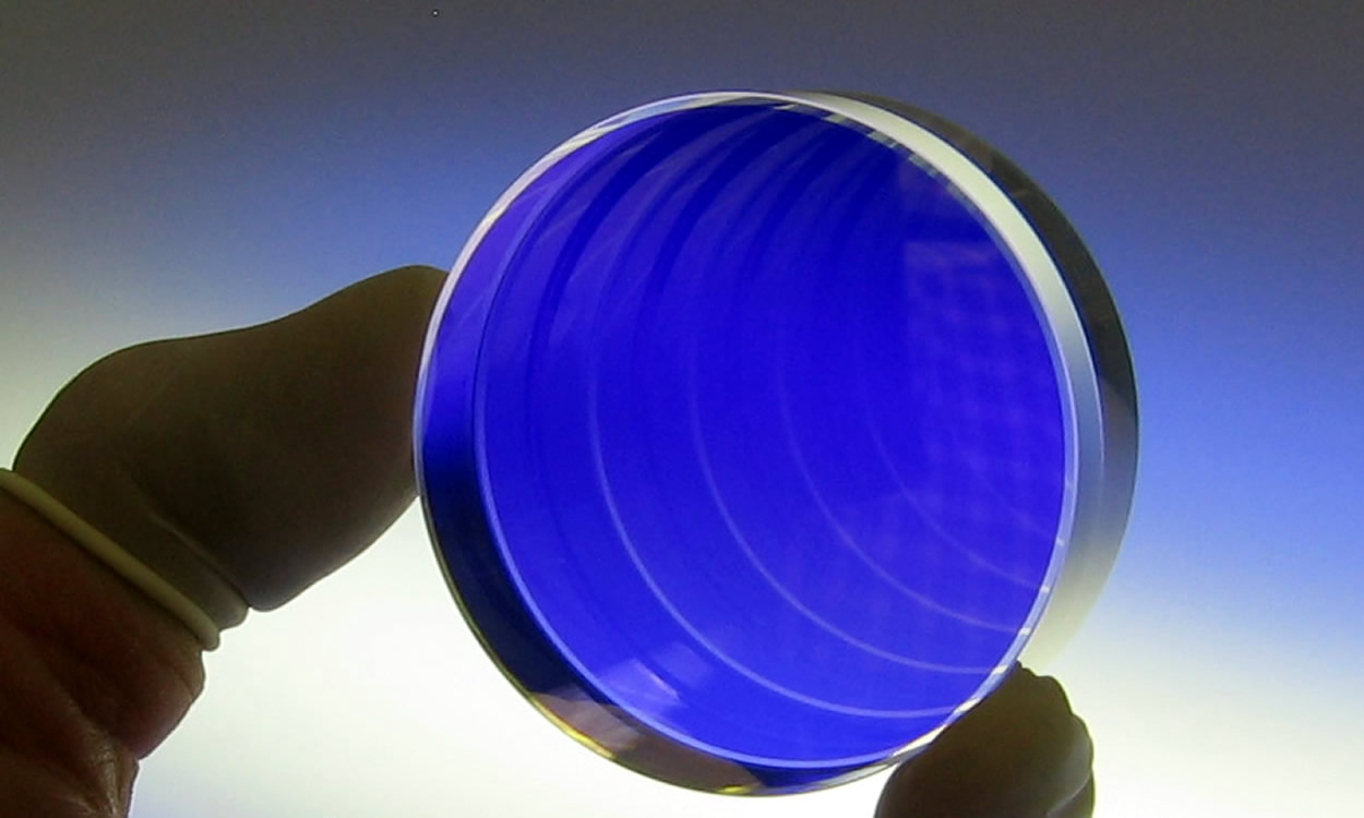
 Measured with tunable laser mapping system in transmission there is a peak to valley slope of about 115nm")


Check out our Catalog and our Calculators!
Optics Catalog
Most of the optics we make are custom made but we still have an interesting catalog. Check it out!
Optical Design Center
Design etalons, lenses, resonators, VIPA's and explore optical material properties.


