Fluid jet polishing is turning the world of optical fabrication upside down. LightMachinery can routinely create near perfect ultra-flat or arbitrary freeform optical components using this cost effective, computer controlled technique.
Fluid Jet Polishing Technology
LightMachinery's patented fluid jet polishing system uses a fine stream of slurry to accurately remove nanometers of material from an optical surface. LightMachinery has spent many years refining this computer controlled polishing technology. While 90% of our optical fabrication is done using conventional techniques, most of our high accuracy etalons, VIPAS, interferometers and wafers are finished using the 'FJP'.
Fluid jet polishing enables LightMachinery to tackle some very complex and difficult optical fabrication tasks with confidence and is opening up a new era of optical device manufacturing.
- The adjustment of the shape and flatness of optical components such as etalon mirrors to within a few nanometers
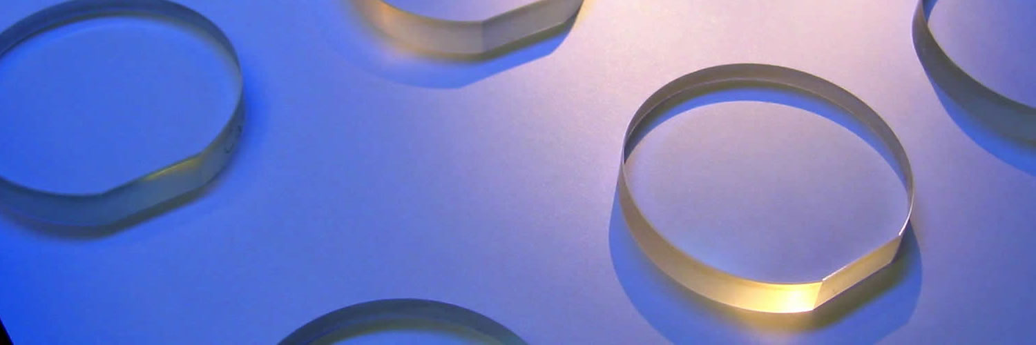
- Very thin components, such as wafers and thin etalons, that are impossible to accurately polish using conventional technology
- The ability to measure the final performance of complex assemblies such as Michelson Interferometers and then to make arbitrary freeform surface corrections to correct the overall performance
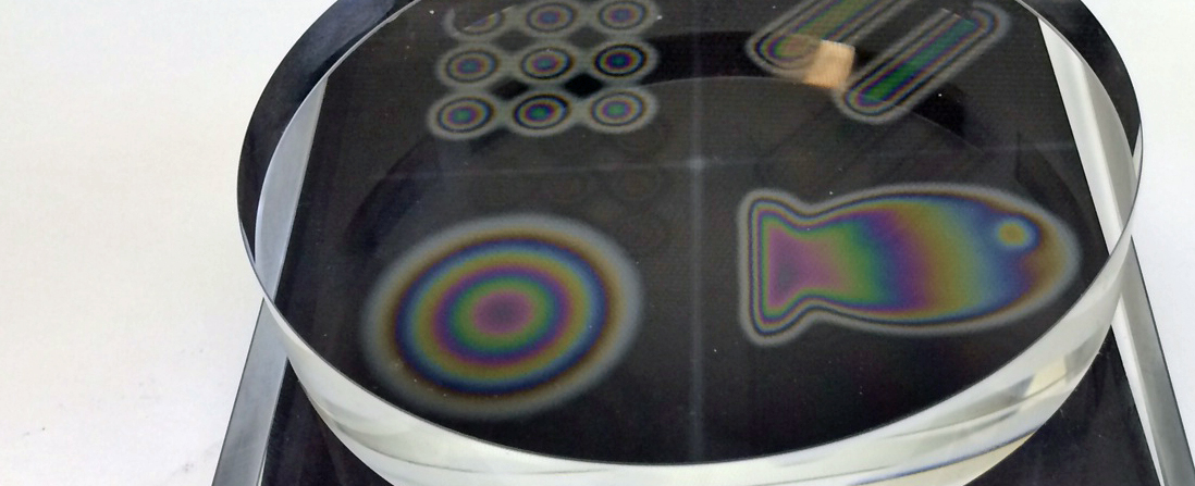
- Arbitrary freeform optical surfaces such as phase plates, corrector plates, axicons and cylindrical axicons
- Materials that are compatible with our FJP process include; Fused Silica, all glasses, crystal quartz, Germanium, Silicon, CaF2, MgF2, Salts
- Non compatible materials (so far) include metals and any material with grain structure or inhomogeneities
FLUID JET POLISHING
More information on the FJP process and some examples too


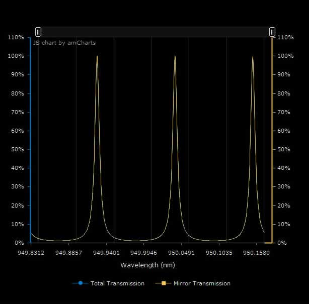
 Measured with tunable laser mapping system in transmission there is a peak to valley slope of about 115nm")


 of the lenses is about 500nm over about 3mm but the radius of curvatures in the central regions of the lenses are about 120cm")


. The depth was set to 250nm for the text.")


 into the square optical component that has then been optically contacted to the lower 3\" diameter holder. The visible fringes are from the air space between the surfaces.")
")


Check out our Catalog and our Calculators!
Optics Catalog
Most of the optics we make are custom made but we still have an interesting catalog. Check it out!
Optical Design Center
Design etalons, lenses, resonators, VIPA's and explore optical material properties.


